Sequential Lamination Process

Sequential Lamination In Pcb Fabrication Camptech Ii Circuits Inc

How To Reduce Pcb Cost With Blind Buried Vias Lisa Chu Pulse Linkedin Stack Stackup Laminate
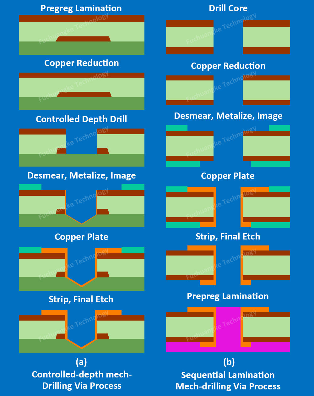
Controlled Depth Mech Drilling Via Process Sequential Lamination Mech Drilling Via Process Pcb

Hdi Pcb Fabrication Basics Fuchuangke Technology Technology Basic Chip Packaging

Speedstack Hdi Sequential Pcb Lamination Plan Youtube

Check Out Here Well Designed Sequential Process To Help Clients Maximize Their Revenue Cyc Revenue Cycle Management Revenue Cycle Health Information Management

Pcb fabricators use any one of four lamination methods.
Sequential lamination process. Sequential lamination also offers the benefits of eliminating any design restrictions or having exposed copper at the routed board edges. Sequential lamination is a variety of technologies where already laminated subparts or subcomposites are laminated to additional layer of copper or another subpart. Sequential lamination technology for high performance multi layer pcbs. Simply put this term describes the process of building up a pcb layer by layer using multiple subcomposites of copper and insulating pcb laminate material this technique allows for the completion of complex tasks such as trace routing on.
A pcb subset is a multilayer printed circuit board presented in an almost completed pcb process. 3 plated closed with electroplated copper. After this a dielectric substance is interposed between each pair of subsets. A sequential lamination process pattern one side laminate to a support layer pattern second side is recommended to minimize material handling issues.
A sequentially laminated printed circuit board pcb goes through at least two lamination cycles and can go through many more. This is due to the nature of the very small drill and the aspect ratio requirement on all drills example 10 1 down to the inner layer. By fabricating a layer with blind vias as if a 2 sided pcb is being made. 2 filled with non conductive or conductive material other than copper as a separate processing step.
The backbone of pcb fabrication the most fundamental manufacturing technique in modern pcb fabrication is sequential lamination. Sequential lamination will result in scaling factors. Sequential lamination of pcb layers is required in order to connect outer surface vias. This build approach is the.
4 screen printed closed with a copper paste. The subsets of the multi layer pcbs are created in separate processes. 1 filled with epoxy resin b stage during a sequential lamination process step. Fabrication entails more than 100 process steps.
It can have benefits for both signal integrity shorter vias and give more flexibility. This process is usually associated with via in pad technology when routing fine pitch densely routed designs. Process control is also critical. Power design services uses advanced sequential lamination technology allowing the manufacture of printed circuit boards pcb as the composition of different subsets of boards and layers.
By taking the pcb multiple times through the production process boards can be built with drilled holes that only appear to go through parts of the stack the process for this type of complex stackup is called sequential lamination. The sequential lamination process involves inserting a dielectric between a layer of copper and an already laminated sub composite. Foil lamination mass lamination sequential. Blind and buried vias can be built into a pcb using sequential lamination.

Sequential Lamination Of High Density Interconnect Hdi Circuits Synergise Pcb Inc
Pcb Stackup Or Buildup A Brief History

An Introduction To The Pcb Lamination Process By Pcbgogo

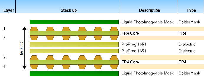
Stack Up Impedance Control 002

Hdi Fabrication Basics Altium Com

Plc Ladder Logic For Sequential Motor Control Study About Plc Motor Programming Tutorials And Implement Plc Ladde Ladder Logic Sequential Programming Tutorial

The Clear And Sequential Process Used For Touchmath Division Continues To Build Upon Previously Learned Skills And Str Touch Math Math Curriculum Math Concepts
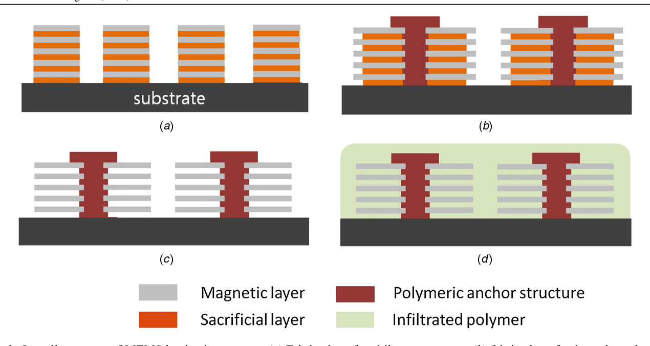
Pdf A Mems Lamination Technology Based On Sequential Multilayer Electrodeposition Semantic Scholar
How 3d Printers Work Simple Google Search 3d Printing Service 3d Printing Projects 3d Printing

Sequence Poster Transition Words Teaching Writing Nonfiction Texts

Writing Center Intermediate Bundle Tickled Pink In Primary Classroom Writing Classroom Writing Center Writing Center

Nclex Rn Study Guide Pediatric Nursing Pediatrics Nursing School Prerequisites

Scarecrow Third Grade Writing 3rd Grade Writing Writing Genres

