Semiconductor Laminate Substrate
Polymers In Electronic Packaging Introduction To Semiconductor Substrates Polymer Innovation Blog

Polymers In Electronic Packaging Build Up Films For Flip Chip Semiconductor Substrates Part Three Polymer Innovation Blog
Polymers In Electronic Packaging Semiconductor Substrates For Flip Chip Polymer Innovation Blog

Substrates For Semiconductor Packaging

How To Measure Tactile Pressure Easy And Precise Pressure Profile Visualization Keywords Printed Circuit Board Manu Printed Circuit Board Circuit Board Fuji

The Advantages Of Thin Film Solar Panels Solar Energy Panels Thin Film Solar Panels Solar Cell

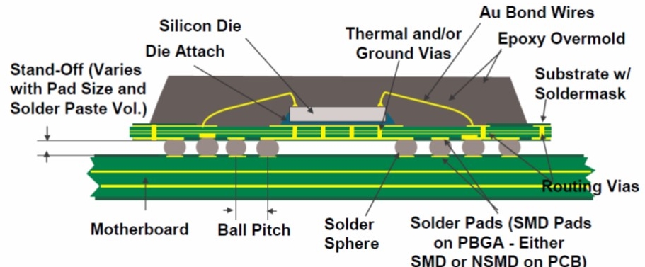
Evenly distributed bumps across the bottom surface of the substrate provide the electrical connection to the system board.
Semiconductor laminate substrate. Ceramic substrates are based on aluminum oxide aluminum nitride and other materials. In total revenues the laminate substrate market is forecasted to reach 10 3 billion in revenues for 2012. Ceramic based packages are used for surface mount devices cmos image sensors and multi chip modules. The difference is that the substrate size is much smaller than most of the pcbs you have seen.
The main reason for this high value is the growth of flip chip substrates which are typically more expensive than wirebond packages. It undergoes many microfabrication processes such as doping ion. Access success in industrializing via post technology in coreless substrate production has broken the monopoly of leading global ic substrate manufactures and is seen as a major breakthrough in substrate development for china s semiconductor industry moving made in china to innovated in china. A compound semiconductor laminate substrate comprising two single crystalline compound semiconductor substrates directly bonded together and laminated the single crystalline compound semiconductor substrates having the same composition including a and b as constituent elements and having the same atomic arrangement characterized in that the front and back surfaces of the laminate substrate.
Substrate layout design rules varies from different suppliers. Magnetic and ferroelectricity film substrate. Substrates can be made by different materials. Substrate design consists of layout of all signals from the package external balls to the bump pads.
We present the advanced coreless laminate substrates in this paper including 3 layer thin substrate built by ets embedded trace substrate technology 3 layer sutc simmtech ultra thin substrate with carrier for fan out chip last package and 3 layer coreless substrate with hsr high modulus solder resist for reduced warpage. Laminate build up ceramic and more. Laminate packages employ a bga design which utilizes a plastic or tape laminate substrate over a leadframe substrate and places the electrical connections on the bottom of the package rather than around the perimeter. Evident by the hundreds of billion units shipped each year leadframes remain a key substrate technology for packaging semiconductors.
Meanwhile substrate based packages fall into several categories such as ceramic and organic laminate. In electronics a wafer also called a slice or substrate is a thin slice of semiconductor such as a crystalline silicon c si used for the fabrication of integrated circuits and in photovoltaics to manufacture solar cells the wafer serves as the substrate for microelectronic devices built in and upon the wafer.
Polymers In Electronic Packaging Build Up Films For Flip Chip Semiconductor Substrates Part One Polymer Innovation Blog

Spi Laser Inverter Circuit Board Buy Online In 2020 Circuit Board Electronics Circuit Circuit

Keywords Photovoltaic Manufacturing Quality Control Vacuum Lamination Tactile Pressure Distribution Measurement S Photovoltaic Manufacturing Direct Method
Semiconductor Laminating Fralock

Semiconductor Electronics Concept Map Mtg Physics For You Magazine Jeemain Jeeadvanced Class11 Classxi Cla In 2020 Physics Concepts Physics Classroom Learn Physics
Semiconductor Fabrication Packaging Materials Dupont

Searching For Pcb Fabrication Supplier What Should They Offer Printed Circuit Boards Substrate Printed Circuit

Triac Pinout And Symbol Electronic Circuit Projects Electronics Projects Diy Electronics

How To Make Wireless Ac Voltage Detector Pen Non Contact Electrical Tester In 2020 Electronics Projects For Beginners Electronics Projects Electrical Tester

Motors Basics Finally How To Use An H Bridge Electronics Projects Electronic Engineering Being Used

The Best Diy Projects Are The Ones That Are Useful Like The Clock We Built Last Time I Had Lots Of Fun Diy Electronics Cool Diy Projects Electronics Projects

Laminate Fr4 Pi Board Thickness 1 57mm Copper Thickness 17 5um Hoz Solder Resist Green Color Surface Finish Immersion Flex Printed Circuit Boards Layers

All About Prefixes Prefixes Writing Words Reading Writing

